 www.LED
The Light Emitting Diode
or short known as LED, is an electronic semiconductor -element with a p-n junction.
PLEASE NOTE!!!:
Our German sites are much more detailed then our English sites. So please switch in our Germen sites and use the language translater (top right) with 60 languages.
If current flows into passage direction by the diode, then it radiates light with a wavelength dependent on the semiconductor material.
 At the beginning of the development of semiconductors, stood one scientific discovery, which was for a long time ignored.1876 Ferdinand Brown hold a lecture on current flow in crystals.
 The first transistor, 1947 The conductivity of a pure semiconductor crystal is based on the formation of freely mobile charge carriers: Electrons and electron holes. The electron holes behave like positive charges. The conductivity increases with increasing temperature. |
Also the second half 20. century is clearly shaped by the upswing of the semiconductor industry. Electronic circuits revolutionized the working sphere and spare time.
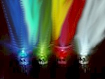
LED´s
, the light of the future| Aluminiumgalliumarsenid (AlGaAs) – red and infrared, till 1000 nm wavelength Galliumaluminiumarsenid (GaAlAs) – 665 nm, red, LWL till 1000 nm Galliumarsenidphosphid (GaAsP) and Aluminiumindiumgalliumphosphid (AlInGaP) – red, orange and yellow Galliumphosphid (GaP) – green Indiumgalliumnitrid (InGaN)/Galliumnitrid (GaN) – UV, blue and green Copperplumbid (CuPb) - emit near Infrared (NIR) White LEDS are mostly blue LEDS with a phosphorus layer, which works as a luminescence converter 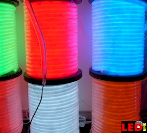 Indiumgalliumnitrid (InGaN)/Galliumnitrid (GaN) – UV, blue, Galliumphosphid (GaP) – green, Galliumaluminiumarsenid (GaAlAs) – z. B. 665 nm, red, Aluminiumindiumgalliumphosphid (AlInGaP), orange. |
By installation a fives valency foreign atoms (donors) we receive more electrons (n - type) and by installation a three valency foreign atoms (acceptors) we receive less electrons (p - type).
We assemble a diode now in thoughts.
We take one piece each of n - type and p - type material. As long as the two pieces do not touch themselves, they are electrically neutral. In the n - type are many freely mobile electrons and in the p - type are many freely mobile electron holes.
Now we bring n and the p - type in contact and apply a current. At the contact area now some comes in motion. Electrons from the n-range and electron holes from the p-range move by the p-n junction (gold lead) and
That means: Electrons are caught by the holes and bound again to lattice sites. The energy freed thereby is radiated as light.
The color of the radiated light depends thus on the material (semiconductor) the Led's.
A new procedure announces a more economical production with white LEDs:
With that most usual manufacturing processes around white LEDs to manufacture, gallium nitride is steamed then again replaced on a bottom layer made of sapphire and again vaporized. Thus develops the first layer GaN semiconductor crystal. In a new procedure of the Birck Nanotechnology center at the University of Purdue the expensive sapphire layer was replaced now by silicon. A coating from zircon nitride prevents that the silicon layer absorbs light. The use of zircon nitride only made possible by one the silicon with an intermediate layer from aluminum nitride covered before, in order to prevent the reaction of the silicon with the zircon nitride. As last layer the gallium nitride becomes vapour-deposited. The substantially more favorable and wide silicon wafers can be used by this procedure for the LED production.
| AGB Ledshift | LED Function | LED Producer | LED Distributor | LED Events | LED Company Entry | LEDS | Sitemap | Contact | |
|
|
© Markus Kottas, Heldenberg Ltd.2018